Step 1: The silicon dioxide of either quartzite gravel or crushed quartz
is placed into an electric arc furnace. A carbon arc is then applied to
release the oxygen. The products are carbon dioxide and molten silicon.
This simple process yields silicon with one percent impurity, useful in
many industries but not the solar cell industry.
Step 2: The 99 percent pure silicon is purified even further using the
floating zone technique. A rod of impure silicon is passed through a
heated zone several times in the same direction. This procedure "drags"
the impurities toward one end with each pass. At a specific point, the
silicon is deemed pure, and the impure end is removed.
Step 3: Solar cells are made from silicon boules, polycrystalline
structures that have the atomic structure of a single crystal. The most
commonly used process for creating the boule is called the Czochralski
method. In this process, a seed crystal of silicon is dipped into melted
polycrystalline silicon. As the seed crystal is withdrawn and rotated, a
cylindrical ingot or "boule" of silicon is formed. The ingot withdrawn
is unusually pure, because impurities tend to remain in the liquid.

Step 4:From the boule, silicon wafers are sliced one at a time using a
circular saw whose inner diameter cuts into the rod, or many at once
with a multiwire saw. (A diamond saw produces cuts that are as wide as
the wafer—. 5 millimeter thick.) Only about one-half of the silicon is
lost from the boule to the finished circular wafer—more if the wafer is
then cut to be rectangular or hexagonal. Rectangular or hexagonal wafers
are sometimes used in solar cells because they can be fitted together
perfectly, thereby utilizing all available space on the front surface of
the solar cell.
Step 5:The wafers are then polished to remove saw marks. (It has recently been
found that rougher cells absorb light more effectively, therefore some
manufacturers have chosen not to polish the wafer.)
Step 6: The traditional way of doping (adding impurities to) silicon
wafers with boron and phosphorous is to introduce a small amount of
boron during the Czochralski process in step #3 above. The wafers are
then sealed back to back and placed in a furnace to be heated to
slightly below the melting point of silicon (2,570 degrees Fahrenheit or
1,410 degrees Celsius) in the presence of phosphorous gas. The
phosphorous atoms "burrow" into the silicon, which is more porous
because it is close to becoming a liquid. The temperature and time given
to the process is carefully controlled to ensure a uniform junction of
proper depth. A more recent way of doping silicon with phosphorous is to
use a small particle accelerator to shoot phosphorous ions into the
ingot. By controlling the speed of the ions, it is possible to control
their penetrating depth. This new process, however, has generally not
been accepted by commercial manufacturers.

Step 7: Electrical contacts connect each solar cell to another and to
the receiver of produced current. The contacts must be very thin (at
least in the front) so as not to block sunlight to the cell. Metals such
as palladium/silver, nickel, or copper are vacuum-evaporated This
illustration shows the makeup of a typical solar cell. The cells are
encapsulated in ethylene vinyl acetate and placed in a metal frame that
has a mylar backsheet and glass cover. This illustration shows the
makeup of a typical solar cell. The cells are encapsulated in ethylene
vinyl acetate and placed in a metal frame that has a mylar backsheet and
glass cover. through a photoresist, silkscreened, or merely deposited on
the exposed portion of cells that have been partially covered with wax.
All three methods involve a system in which the part of the cell on
which a contact is not desired is protected, while the rest of the cell
is exposed to the metal.
Step 8: After the contacts are in place, thin strips ("fingers") are
placed between cells. The most commonly used strips are tin-coated
copper
Step 9: Because pure silicon is shiny, it can reflect up to 35 percent
of the sunlight. To reduce the amount of sunlight lost, an
anti-reflective coating is put on the silicon wafer. The most commonly
used coatings are titanium dioxide and silicon oxide, though others are
used. The material used for coating is either heated until its molecules
boil off and travel to the silicon and condense, or the material
undergoes sputtering. In this process, a high voltage knocks molecules
off the material and deposits them onto the silicon at the opposite
electrode. Yet another method is to allow the silicon itself to react
with oxygen- or nitrogen-containing gases to form silicon dioxide or
silicon nitride. Commercial solar cell manufacturers use silicon
nitride.
Step 10: he finished solar cells are then encapsulated; that is, sealed
into silicon rubber or ethylene vinyl acetate. The encapsulated solar
cells are then placed into an aluminum frame that has a mylar or tedlar
backsheet and a glass or plastic cover.

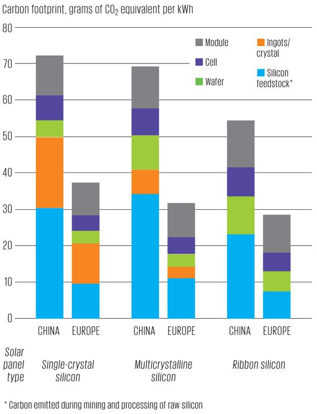
Studies show that production takes more resources than accounted for. Pollution, transport, installation and
recycling are often not very documented. Also it differs on the location of production and deployment. Waste of
production includes toxic elements, pollution of clean water, mining operations. Depending on the case solar
panels can be beneficial (*1)
Solar energy is largely subsidized. Because of this it gets beneficial to consumers. The drawback is that the
price is not a measurement of real cost of production (and possibly use of resources). (*2)
- Solar energy isn't always as green as you think
- The true cost of solar energy